
Test Engineering. Failure Analysis. Answers.
info@datest.com
|
(+1) 510.490.4600

Flying Probe Testing is a precise, non-invasive method for identifying connectivity faults and verifying functionality in complex PCBAs. Ideal for prototypes and low- to medium-volume production, it enables rapid program development and high-accuracy testing for dense, multi-layer boards.

Datest utilizes advanced SPEA flying probe systems to deliver complete solutions, from in-house testing and custom program development to coverage analysis and on-site implementation. With high-speed performance (up to 160 tests/second) and ultra-fine probing capability (down to 50 microns), we help you achieve reliable results quickly, without the cost and lead time of fixtures.

SPEA Logo

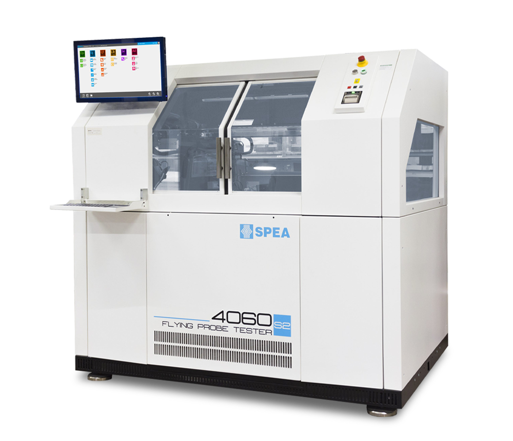
SPEA 4060 S2 Dual-Sided Flying Probe with LED & High-Density Wafer Test Capability

SPEA 4060

What Flying Probe Catches

No fixtures. No guesswork. Just precise, point-to-point testing that finds the defects hiding in your boards.

Open Circuits

Missing or broken traces, incomplete solder joints, or defective vias that cause loss of continuity.

Short Circuits

Solder bridges, unintended connections between traces or components that can cause failures.

Solder Joint Defects

Cold solder joints, insufficient solder, or tombstoning (especially with small passives like resistors and capacitors).

Incorrect Component Values

Resistors, capacitors, and inductors with incorrect values compared to the design specifications.

Misaligned or Missing Components

Incorrectly placed, rotated, or completely missing components that can affect functionality.

Programming

Bridging the Gap in Test Expertise

Programming Fell Behind? Yeah… That Happens.

Flying probe programming isn’t easy, and when your expert disappears or bandwidth gets tight, production feels it fast. That’s where Datest steps in.

We build, optimize, and support custom programs for SPEA systems (4020–4080), delivering reliable coverage without the need for in-house resources. New programs, updates, coverage analysis, we keep your test process moving, accurate, and under control.

Key Benefits

Effective for High-Density and Complex Multi-Layer PCBs

FPT can access tight areas and fine-pitch components that may be difficult for ICT fixtures, making it ideal for modern, high-density board designs. Additionally, it can test multiple layers and detect shorts or opens within complex PCB designs, providing thorough coverage for multi-layer boards that might not be fully testable with visual inspection alone.

Fast and Easy Test Program Development

Unlike in-circuit testing (ICT), which requires expensive bed-of-nails fixtures, FPT uses programmable probe movements, since FPT relies on software-driven test routines rather than custom hardware, it allows for quick setup and program modifications, making it ideal for early design validation.

Flexibility for Design Changes

Since test probes are programmable, FPT can accommodate design modifications without requiring hardware changes, which is particularly useful in R&D and prototyping environments.

Ideal for Low-to-Medium Volume Production

Since test probes are programmable, FPT can accommodate design modifications without requiring hardware changes, which is particularly useful in R&D and prototyping environments.

Not Sure What Test You Need?

That’s kind of our thing.

Most customers don’t come to us knowing exactly which test will solve their problem. They come with a failure, a requirement, a deadline, or a part that “just isn’t behaving.”

That’s where Datest comes in.

Understand what’s actually going on

Determine which test methods make sense (and which don’t)

Avoid unnecessary testing, cost, and delays

Build a clear, defensible path forward

No guesswork. No pressure. Just honest guidance from people who do this every day.